LVDS PCB Layout – Expert Guidelines You Need to Know! The 13 most used pcb layout design tools
If you are searching about How to Design PCB Layout? - Guidelines, Advantages and Disadvantages you've visit to the right web. We have 25 Pictures about How to Design PCB Layout? - Guidelines, Advantages and Disadvantages like AN11088 LVDS Design Guidelines | PDF | Printed Circuit Board | Computer, LVDS Detail | PDF and also Some LVDS PCB Layout Guidelines for Ensuring Signal Integrity | PCB. Here it is:
How To Design PCB Layout? - Guidelines, Advantages And Disadvantages
 compuinfohub.blogspot.com
How to Design PCB Layout? - Guidelines, Advantages and Disadvantages ...
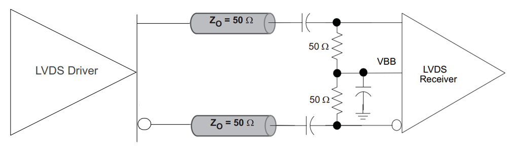
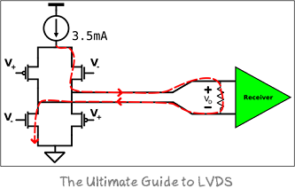
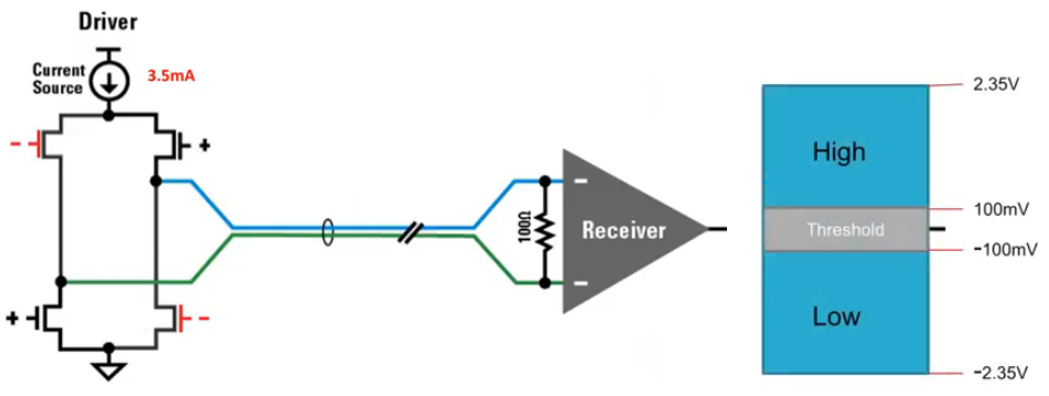
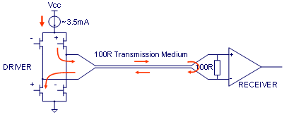
Some LVDS PCB Layout Guidelines For Ensuring Signal Integrity | PCB
 resources.altium.com
Some LVDS PCB Layout Guidelines for Ensuring Signal Integrity | PCB ...
Some LVDS PCB Layout Guidelines For Ensuring Signal Integrity | PCB
Some LVDS PCB Layout Guidelines for Ensuring Signal Integrity | PCB ...
AN11088 LVDS Design Guidelines | PDF | Printed Circuit Board | Computer
 www.scribd.com
AN11088 LVDS Design Guidelines | PDF | Printed Circuit Board | Computer ...
Top PCB Design Guidelines Every PCB Designer Needs To Know | Altium
 www.pinterest.co.uk
Top PCB Design Guidelines Every PCB Designer Needs to Know | Altium ...
PCB Layout Guidelines.pdf
 www.slideshare.net
PCB Layout guidelines.pdf
Some LVDS PCB Layout Guidelines For Ensuring Signal Integrity | PCB
 resources.altium.com
Some LVDS PCB Layout Guidelines for Ensuring Signal Integrity | PCB ...
Top 5 PCB Design Rules You Need To Know | PCB Design Blog | Altium
 resources.altium.com
Top 5 PCB Design Rules You Need to Know | PCB Design Blog | Altium
PCB Layout Rules For PCIE, SATA, LAN, LVDS, USB, SDVO,
 www.fedevel.com
PCB layout rules for PCIE, SATA, LAN, LVDS, USB, SDVO,
Some LVDS PCB Layout Guidelines For Ensuring Signal Integrity | PCB
Some LVDS PCB Layout Guidelines for Ensuring Signal Integrity | PCB ...
LVDS Interface And PCB Layout Requirments - Intel Community
 community.intel.com
LVDS Interface and PCB layout requirments - Intel Community
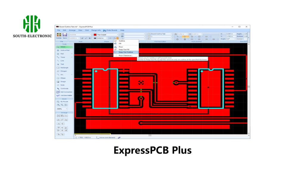
The 13 Most Used PCB Layout Design Tools
 southelectronicpcb.com
The 13 Most Used PCB Layout Design Tools
LVDS: High Speed LVDS PCB Design Guidelines | MADPCB
 madpcb.com
LVDS: High Speed LVDS PCB Design Guidelines | MADPCB
Practical PCB Design Layout Rules - Leading PCB Manufacturer - Arisentec®
 arisentecpcb.com
Practical PCB design layout rules - Leading PCB Manufacturer - Arisentec®
All LVDS PDF | PDF
 www.scribd.com
All LVDS PDF | PDF
Some LVDS PCB Layout Guidelines For Ensuring Signal, 40% OFF
 www.oceanproperty.co.th
Some LVDS PCB Layout Guidelines For Ensuring Signal, 40% OFF
Some LVDS PCB Layout Guidelines For Ensuring Signal, 40% OFF
 www.oceanproperty.co.th
Some LVDS PCB Layout Guidelines For Ensuring Signal, 40% OFF
Some LVDS PCB Layout Guidelines For Ensuring Signal, 40% OFF
 www.oceanproperty.co.th
Some LVDS PCB Layout Guidelines For Ensuring Signal, 40% OFF
LVDS2 - Geekworm Wiki
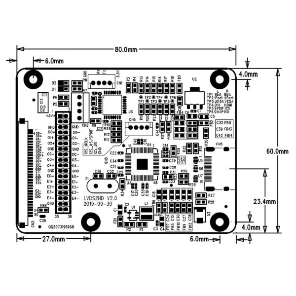 wiki.geekworm.com
LVDS2 - Geekworm Wiki
PCB Design Layout Guidelines For Engineers | Advanced PCB Design Blog
 resources.pcb.cadence.com
PCB Design Layout Guidelines for Engineers | Advanced PCB Design Blog ...
Some LVDS PCB Layout Guidelines For Ensuring Signal Integrity | PCB
 resources.altium.com
Some LVDS PCB Layout Guidelines for Ensuring Signal Integrity | PCB ...
LVDS Detail | PDF
 www.scribd.com
LVDS Detail | PDF
A Detailed Guide To PCB Layout Design - IBE Electronics
 www.pcbaaa.com
A detailed guide to PCB layout design - IBE Electronics
Layout PCB Inverter: Tips And Best Practices For Successful Design
 hillmancurtis.com
Layout PCB Inverter: Tips and Best Practices for Successful Design ...
Expert PCB Layout Services -PCBA One-stop Solution
 hilelectronic.com
Expert PCB Layout Services -PCBA One-stop Solution
Some lvds pcb layout guidelines for ensuring signal, 40% off. Lvds interface and pcb layout requirments. Some lvds pcb layout guidelines for ensuring signal, 40% off